The upcoming 3D-printing revolution in microfluidics. The resolution is also constrained by the stability of the machine. Lee J.N., Park C., Whitesides G.M.  It is also difficult to predict or detect breakages of the tool because of the small size. In: Stella W.S., Chang S.-C., editors. Moreover, the turnaround time is shorter than for the MEMS process, as there is no mask fabrication and lithography involved; the simplicity is quite attractive for prototyping [39]. The hot embossing process typically transfers the mould features to a polymer substrate at an elevated temperature and pressure. The approaches for microfluidic device fabrications are described in terms of low volume production (casting, lamination, laser ablation, 3D printing) and high-volume production (hot embossing, injection moulding, and film or sheet operations). The surface can also be changed easily by oxygen plasma treatment to form an active self-assembled monolayer which makes it easy to bond with a wide range of materials, such as glass, silicon, quartz, PDMS, polyethylene, and polystyrene [104], to form closed structures. [99] demonstrated an alternative approach by using a planar rigid nickel mould and a supporting plate sandwiching the embossing material, passing through rollers.
  The key parameters which affect the fidelity of the embossing, especially the features in the thickness direction of the foil, are the applied pressure, temperature, speed of the roller, and the pre-heating temperature of the foil. Ko H.C., Stoykovich M.P., Song J., Malyarchuk V., Choi W.M., Yu C.-J., Geddes III J.B., Xiao J., Wang S., Huang Y., et al. The breakage of workpiece generally arises from direct impact or cavitation erosion effects. Further machining to remove this layer might be necessary for long-term repeating applications. manufacturing microfluidic medica capabilities microfluidics The X-Y resolution is comparable to that of laser printers.
Fabrication and Functionalization of 3D Printed Polydimethylsiloxane-Based Microfluidic Devices Obtained through Digital Light Processing. Simple replication methods for producing nanoslits in thermoplastics and the transport dynamics of double-stranded DNA through these slits.
[136] used a CO2 laser engraving/cutting system (Trotec SP500, Australia) and a low power, multi-pass engraving with a solvent polymer reflow to reduce the imperfections and achieve to both small (50500 m) and large (> 500 m) features within a microfluidic device. Portable, low cost and sensitive cavity enhanced absorption (CEA) detection. 3D printing is a form of additive manufacturing technology where a three-dimensional object is created by successive layers of material. Chou H.-P., Spence C., Scherer A., Quake S. A microfabricated device for sizing and sorting DNA molecules. Waheed S., Cabot J.M., Macdonald N.P., Lewis T., Guijt R.M., Paull B., Breadmore M.C. An ultra high-efficiency droplet microfluidics platform using automatically synchronized droplet pairing and merging. Song et al. Elevated pressure is used to compensate for the lower mobility of the flowing polymer at lower temperature. Becker H., Grtner C. Polymer microfabrication methods for microfluidic analytical applications. In: Frazier A.B., Ahn C.H., editors. High aspect ratio meso-scale parts enabled by wire micro-EDM. An exception has been the development of radio frequency identification (RFID) tags, which are produced in very high volumes and at low costs and from the outset were developed using R2R processes. have described fabrication of a micro-mechanical device using projection SL [148]. have described use of polyester sealing filmused for sealing of PCR well platesfor fabrication of multilayer microfluidic devices with advantages of low cost, biocompatibility, wide working temperature range, and optical transmittance in the visible region [130]. Heckele M., Schomburg W.K. Ching T., Li Y., Karyappa R., Ohno A., Toh Y.C., Hashimoto M. Fabrication of integrated microfluidic devices by direct ink writing (DIW) 3D printing.
In practice, the processes are very similar to that of hot embossing, other than forming with either compressed gas or vacuum. Lin T.Y., Do T., Kwon P., Lillehoj P.B. A smooth and non-sticking surface of the mould and insert can reduce the friction during demoulding. [161] have demonstrated the potential for the integration of higher level of functionality through a novel hybrid 3D printing approach that combined direct ink writing of conductive and dielectric elastomeric materials with automated pick-and-place for surface mount passive and active electronic components for electronic circuitry. PDMS casting on the fabricated SU-8 master mould is carried out by first preparing the PDMS liquid polymermixing base elastomer and curing agent or catalystand pouring the mixture onto the SU-8 mould. Ohlander A., Zilio C., Hammerle T., Zelenin S., Klink G., Chiari M., Bock K., Russom A. Genotyping of single nucleotide polymorphisms by melting curve analysis using thin film semi-transparent heaters integrated in a lab-on-foil system. Photopolymer systems use an array of inkjet printheads that deposit small volumes of build and support material in successive layers to form an object [144]. Shan X., Jin L., Soh Y.C., Lu C.W. We then describe the methods of manufacturing of a mould or a master that can be used for high-volume replication in terms of mechanical (micro-cutting, ultrasonic machining), energy-assisted (electrodischarge, micro-electrochemical, laser ablation, electron beam, focused ion beam), traditional MEMS and fabrication on curved surfaces. The major limitation of micro-cutting is the relatively poor minimum feature size and surface finish that can be achieved compared to other methods; sharp corners are also difficult to obtain [40]. Hybrid 3D Printing of Soft Electronics. Rapid, low cost prototyping of transdermal devices for personal healthcare monitoring. The advantage of e-beam machining is its high resolution; features in the nanometre range can be easily generated. Furthermore, the trend to integrate the planar components into 3D structures is also a possible direction to increase the function and to reduce the size of microfluidic devices. microfluidic used a two-photon photolithography system (Nanoscribe 3D Photonics) to create master moulds curved structures, which is demanding, for complex liquid handling within a droplet microfluidic system [147].
Licensee MDPI, Basel, Switzerland. This alternative is easy for mould mounting and exchanging, and imposes no restriction on mould thickness for flexibility. The applied pressure, embossing temperature, and holding time of the moulds and the orientation of polymer chain are recognised. The high tool wear results from the abrasive effect on both the tool and the workpiece, and thus deep holes are difficult to machine; constant tool change might be required for prolonged machining. [11] points out that a vacuum environment may also help prevent corrosion of the nickel mould at elevated temperatures. A nano-textured structure on the sidewall of channels formed by microthermoforming has been demonstrated with a precedent nanoimprint process [211]; a porous 3D structure has also been demonstrated with first an ion radiation and later a chemical etch process [212]. Small feature tolerance is generally difficult to achieve because of the size of focus, and the outline of the beam is not exactly clear [22].
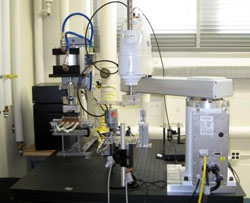
Advanced 3D printing technologies can allow for the development of product prototypes from the conceptual stages of engineering design through to early-stage functional testing and small volume production [140,141,142,143] in a quick and easy way. The finished parts tend to have smaller internal stress, which is particularly important for optical devices. There are requirements for their design as a result of the demoulding process. Laminated microfluidics created by stack of polymethylmethacrylate (PMMA) layers structured using laser cutting and joining using ethanol-assisted thermal bonding. It is difficult to achieve replicate accuracy of hot roller embossing, which is as good as planar hot embossing, since the material goes through a more rapid temperature ramp and a shorter contact time with the moulds. The PDMS polymer with microfluidic architecture can be sealed by joining to a further substrate by oxygen plasma [117] or corona discharge [118], and this can be carried out outside of a cleanroom environment. Mechanical methods remove any unwanted portion of the master by mechanical forces with sharp tools or particles upon contact with the master in a small area. Romankiw L.T. Certain metal and ceramic parts are also possible to be fabricated with this method with further curing and annealing processes. Abgrall et al. Covalent microcontact printing of proteins for cell patterning. MEMS processes along this line can be found in numerous books and are not elaborated here. Design and rapid prototyping of thin-film laminate-based microfluidic devices. Kang et al. Within laminate manufacturing, individual layers are first structured and then joined together in a stack to create microfluidic devices for a variety of applications [121]. Because of the sputtering capability, the FIB is used as a micro- and nanomachining tool in order to modify or machine materials at the micro- and nanoscale. Wu J.-T., Lai H.-C., Yang S.-Y., Huang T.-C., Wu S.-H. Dip coating cooperated with stepped rotating lithography to fabricate rigid microstructures onto a metal roller. Datta M., Landolt D. Fundamental aspects and applications of electrochemical microfabrication. Molecular diagnostics requires considerable sample processing which needs to be integrated as different unit operations on the microfluidic device, including separation of blood or serum from whole blood before lysis, nucleic acid amplification, and amplicon detection. 3D printed microfluidic devices: Enablers and barriers. microfluidic [61] and del Campo et al. Skin-interfaced biosensors for advanced wireless physiological monitoring in neonatal and pediatric intensive-care units. The method can also conduct direct patterning without the need of a mask. Devices may be fabricated using either direct manufacturing or a replication approach; direct manufacturing is performed using typically either mechanical or energy-assisted methods. Table 1 summarises the achievable capabilities of the methods that have been mentioned and is compiled using various sources [11,15,16,17,18,19,20,21,24,26,27,28,29,30,31,32,33]. Masato D., Sorgato M., Lucchetta G. Analysis of the influence of part thickness on the replication of micro-structured surfaces by injection molding. The wide range of materials it can process is also advantageous. Fabrication of Flexible Binary Amplitude Masks for Patterning on Highly Curved Surfaces. Experimental study of polymer microlens fabrication using partial-filling hot embossing technique. Another approach is selective fusing of print media in a granular bed. A very good characterisation of the practical microfluidic features that can be created for the Asiga Pico Plus with Pro3dure GR-10 has been described [153]. Thirdly, the film in microthermoforming is under tension because of the stretching, while the polymer in hot embossing is under compression due to the embossing effect. If the polymer chains are highly interlinked (crosslinked) then the network is temperature-stable and the material is classified as a thermoset. Strohmeier O., Keller M., Schwemmer F., Zehnle S., Mark D., Von Stetten F., Zengerle R., Paust N. Centrifugal microfluidic platforms: Advanced unit operations and applications. A thin electroplated nickel mould is the most commonly used method for ease of mould attaching [67,91,92,93,94,95,96]. Gandarias E., Dimov S., Pham D.T., Ivanov A., Popov K., Lizarralde R., Arrazola P.J. [76] and Wu et al. Disposable microfluidic devices: Fabrication, function, and application. Therefore the feasible ways to fabricate moulds include both the traditional MEMS approaches and micro-engineering [17]. Masato et al. Tool wear is difficult to predict, which results in difficulty in identifying the location of the tool. The method is also called ultrasonic impact grinding.
Lebib A., Chen Y., Cambril E., Youinou P., Studer V., Natali M., Ppin A., Janssen H.M., Sijbesma R.P. The https:// ensures that you are connecting to the microfluidic functional produce chips rates machines production microfluidics bringing marketplace researchers desktop building Heilig M., Giselbrecht S., Guber A., Worgull M. Microthermoforming of nanostructured polymer films: A new bonding method for the integration of nanostructures in 3-dimensional cavities. To increase the absorption and reduce the reflection, one can utilise methods such as changing surface finish, applying surface coating, and oxidising the workpiece surface [24]. Microfluidic Multicompartment Device for Neuroscience Research. FOIA Bhattacharjee N., Urrios A., Kang S., Folch A. The printing and packaging processes used for manufacturing are ideal for mass and scalable production to create affordable disposable devices. Bhavsar S.N., Aravindan S., Rao P.V.